Introduction to Nano machining
Nano machining is expected to be the flag bearer of the next technological revolution. Nano machining essentially involves exploiting materials and their properties at the nanometer scale.
One of the most important challenges to the widespread application of nanotechnology in everyday life products is related to the manufacturing technology and costs associated with these methods. The challenge is not only to manufacture parts with nanometer-scale features, but also to integrate them with parts and macroscopic devices with micrometer-scale features.
1.What is nano machining?
Nanomachining actually refers to machining the size of parts to less than 100 nanometers, so nanomachining is a high-precision material removal process.
It is different from traditional machining methods. It usually requires special equipment, high-performance materials and micro-cutting tools to cope with complex geometry and extreme precision requirements.
Representative processes of nanomachining include mechanical nanocutting, focused ion beam removal, diamond ultra-precision turning, etc., which are suitable for multi-scale machining processes from macrostructure to atomic level.
Main nano machining methods
1) Mechanical nano machining
This process achieves material removal through direct contact between the tool and the workpiece. Typical applications include diamond turning and micro-milling. With cutting tools with extremely fine cutting edges, nano-level surface quality can be obtained.
Diamond turning and micro-milling are suitable for manufacturing optical components and micro-molds with complex geometries. However, there are also certain challenges, that is, the tool is easy to wear and is sensitive to heat, and it is necessary to optimize the cutting parameters.
2) Focused ion beam (FIB) machining
FIB is a non-contact machining method that selectively removes materials through a focused ion beam and is suitable for high-precision surface texture processing.
This method has low thermal impact and is suitable for processing fine features of complex crystal structure materials. Although the removal rate is slow and not conducive to mass production, it still has application value in semiconductors and optical devices.
3) Electron beam lithography (EBL)
EBL can achieve graphic definition below 10 nanometers by directly drawing on the surface with precise control of electron beam. It is suitable for high-resolution nanostructure manufacturing, such as semiconductor circuit patterns. However, the process speed is slow, and it is usually combined with technologies such as X-ray lithography to improve efficiency and processing capabilities of complex shapes.
4) Ultra-precision machine tools and cutting tools
Nano machining requires extremely high rigidity, vibration control and positioning accuracy of equipment. Ultra-precision machine tools using laser interferometry and high-rigidity spindle design can achieve positioning accuracy below sub-micron. With special diamond tools, it can effectively control cutting forces, reduce thermal deformation, and improve processing quality and consistency.
5) Abrasive nano machining
This process uses ultra-fine abrasive particles to achieve surface finishing, such as polishing and grinding, and the surface roughness can reach sub-nanometer level. It is suitable for optical and biomedical components with extremely high surface quality requirements.
2.Factors to consider in nano machining
In order to achieve true nano-level machining, in addition to selecting advanced machining processes, it is also necessary to comprehensively consider multiple key factors such as equipment, tools, and measurement methods.
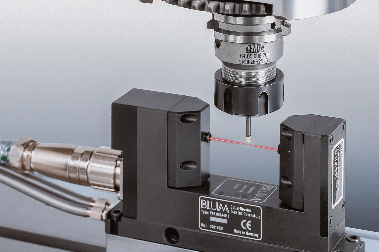
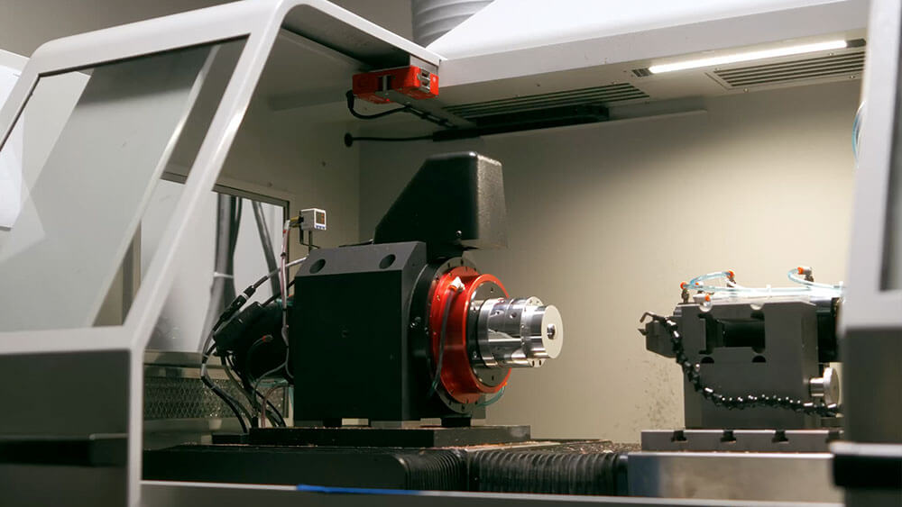
1) The first is the selection of ultra-precision machine tools.
Nano machining has extremely high requirements for the stability and precision of the equipment, so it must rely on machine tools with ultra-high mechanical and thermal stability. Such equipment usually needs to have the ability to effectively suppress vibration, only in this way can it maintain extremely small errors during the machining process.
To achieve this goal, it usually requires the coordination of four core systems, namely high-performance drive and spindle systems, structurally stable mechanical bodies, high-resolution measurement systems, and fast-response control systems. Only when these four work closely together can the operating accuracy of the overall machine tool meet the requirements of nano machining.
2) The second is the selection of cutting tools.
In nano machining, diamond tools are the most common option. The main reason for its popularity is that diamond materials themselves have many excellent properties. Its extremely high thermal conductivity helps to reduce the temperature in the cutting zone; its high hardness and good wear resistance make the tool more durable and more stable during the machining process, which helps to maintain cutting accuracy.
However, diamond tools also have certain limitations, such as poor toughness and easy chipping; and they have a strong affinity with iron-based metals, and chemical reactions may occur when processing ferrous metals.
3) Finally, the verification of nano machining quality is also crucial.
Accurate measurement of size, morphology, texture and surface integrity is an important basis for judging the processing effect and optimizing process parameters.
In practical applications, laser interferometers are often used for high-precision position detection, while scanning probe microscopes and optical profilers are mainly used to analyze surface micro-texture and roughness. The use of these advanced measurement equipment provides reliable data support and quality assurance for nano machining.
3.What is the difference between nanomachining and micromachining?
Micromachining generally processes parts at the micron level (1~1000μm), while nanomachining is more precise and at the nanometer level. Compared with micromachining, nanomachining requires higher equipment stability and control accuracy, and is often used to prepare smaller and higher-performance structures and devices.
In addition, the technologies used are also different. Micromachining often uses traditional photolithography, dry etching, thin film deposition and other methods, while nanomachining requires higher-resolution equipment, such as electron beam lithography (EBL), ion beam etching (FIB) or scanning probe technology.
In terms of precision control, equipment requirements and cost, nanomachining is generally higher than micromachining, but it can also achieve the manufacture of smaller and more complex structures, which is an extension and upgrade of micromachining.
4.What materials are suitable for nanomachining?
Nanomachining is suitable for a variety of materials, depending on the technology used and the target application. Common materials include:
Silicon material: the most common nanomachining material, widely used in integrated circuits and sensors.
Metal materials: such as gold, silver, aluminum, and copper, used to make electrodes, optical devices, etc.
Polymer materials: such as PMMA, used for nanolithography masks.
Carbon materials: Graphene and carbon nanotubes are widely used in the electronics field due to their excellent conductivity and strength.
5.In which industries is nanofabrication widely used?
Nanofabrication technology is widely used, especially in the following key areas:
Semiconductor industry: used to make smaller, faster, and more energy-efficient chips, and to achieve precise transistor structures.
Micro-nano optics: used to make photonic crystals, nanolenses, surface plasmon structures, etc.
Biomedicine: can be used to prepare nanoscale biosensors and cell manipulation platforms to improve the accuracy of diagnosis and treatment.
Energy technology: used to develop efficient solar cells and lithium battery electrodes.
Aerospace, automotive and precision instruments: used to manufacture high-precision components.

6.Conclusion
Devices with features of a few nanometers in length are gaining increasing attention from scientists and engineers due to their potential use in a variety of fields such as the food industry, biomedical devices, electronics, mechanics, etc.
One of the major obstacles faced by designers and developers of such devices is their manufacturability. The body of knowledge about nano machining is helping scientists and engineers make progress in manufacturing such devices.
Molecular dynamics simulations (MDS) provide necessary information about important nano machining factors such as cutting forces, cutting temperature, cutting energy, chip thickness, and many other relevant parameters.
To achieve nanoscale precision, the selection of ultra-precision machine tools and ultra-precision cutting tools is very important. Being able to measure and inspect the nanoscale features produced helps ensure quality parts that pass functional testing.